CPU in 40 lines of SV
This project builds a small 16-bit CPU in five incremental steps. Each step is complete, and adds only few new lines. Programs are written directly in SV testbench. Full CPU here.
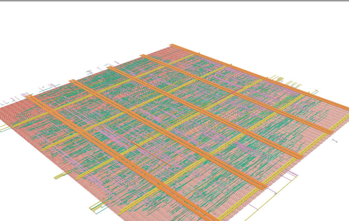
Interactive 3D preview unavailable in this browser. Open the GLB file directly.
Quickstart
make fresh     # if you havent started the container
make enter     # to enter the running container

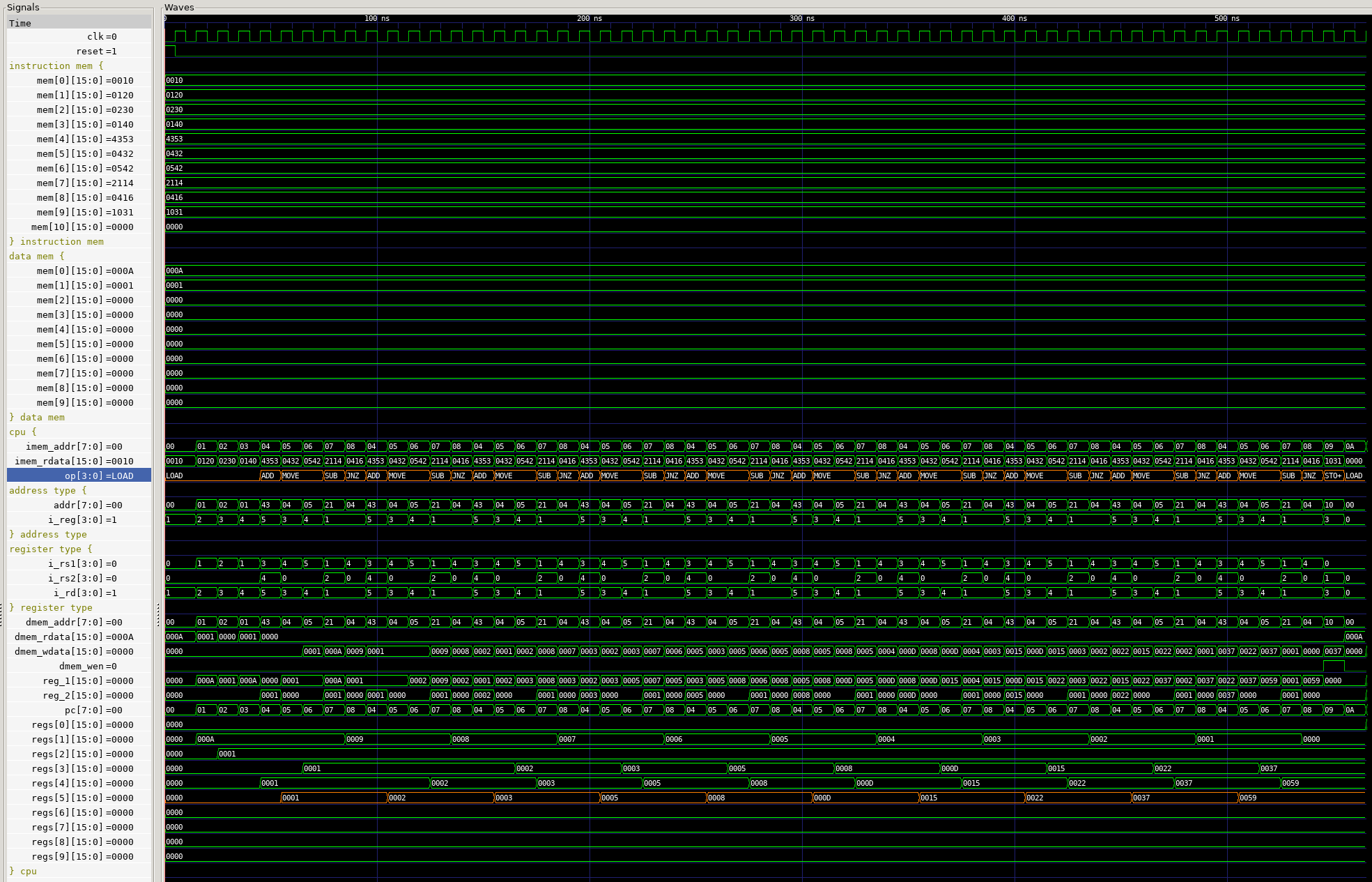
make sim gtkwave DESIGN=cpu_3_store_data      # simulate the step 3 design & view waveform
# Ctrl+C to exit gtkwave

make sim gtkwave DESIGN=cpu_factorial         # run factorial on the final CPU

make gds show_layout DESIGN=cpu_factorial     # Run GDS flow
Example programs:
Incremental evolution
Level |
Feature |
RTL |
|---|---|---|
|
Simple memory with zero-latency read and 1-cycle-latency write |
|
|
Just a counter to load instructions (PC) |
|
|
Sixteen registers and |
|
|
|
|
|
|
|
|
|
CPU Design
Only 8 opcodes:
NOP=0,LOAD=1,STORE=2,MOVE=3,ADD=4,SUB=5,MUL=6, andJNZ=7.NOPis the all-zero instruction and has no side effects.Two instruction formats:
Address type:
LOAD, STORE, JNZtake a data-memory address (addr) and register index (i_reg_a)Register type:
MOVE, ADD, SUB, MULtake indices of three registers. Two sources (i_reg_b, i_reg_c) and one destination (i_reg_a).
JNZjumps toaddrwhenregs[i_reg_a]is nonzero.
| Instructions | Format | 4 Bits [15:12] | 4 Bits [11:8] | 4 Bits [7:4] | 4 Bits [3:0] |
|---|---|---|---|---|---|
LOAD, STORE, JNZ |
Address | addr |
i_reg_a |
opcode |
|
MOVE, ADD, SUB, MUL |
Register | i_reg_c |
i_reg_b |
i_reg_a |
opcode |
Reading Instructions
Each instruction field is 4-bits, so it becomes a character when displayed as hex, making it easy to read binary. Read right to left (little endian). e.g.
0x 1251 : 1=LOAD regs[5] <- dmem[0x12]
0x 0124 : 4=ADD  regs[2] <- regs[1] + regs[0]
Example: Sum to N numbers
The algorithm described in C:
// setup:
uint16_t mem[256];
mem[0] = 0;    // sum seed
mem[1] = 1;    // the constant one
mem[2] = 10;   // N

// run:
uint16_t r0_sum   = mem[0];
uint16_t r1_one   = mem[1];
for (r2_count = mem[2]; r2_count !=0; r2_count -= r1_one) {
  r0_sum += r2_count;
}
mem[4] = r0_sum;  //55
The algorithm described in our machine code and assembly:
0: R0_SUM     = *(0);
1: R1_ONE     = *(1);
2: R2_COUNTER = *(2);
3: R0_SUM     = R0_SUM + R2_COUNTER;
4: R2_COUNTER = R2_COUNTER - R1_ONE;
5: if (R2_COUNTER != 0) goto 3;
6: *(4) = R0_SUM;
Full CPU (40 LOC)
module cpu (
  input  logic        clk, reset,
  output logic [7 :0] pc,          addr,
  input  logic [15:0] instruction, read_data,
  output logic [15:0] write_data,
  output logic        dmem_wen
);
  enum logic [3:0] {NOP, LOAD, STORE, MOVE, ADD, SUB, MUL, JNZ} opcode;
  logic [ 3:0] i_reg_a, i_bus_b, i_bus_c;
  logic [15:0][15:0] regs;
  logic [15:0] bus_a, bus_b, bus_c, alu_out;
  logic reg_wen, jump;

  always_comb begin
    {addr,             i_reg_a, opcode} = instruction;
    {i_bus_c, i_bus_b, i_reg_a, opcode} = instruction;

    bus_a      = regs[i_reg_a];
    bus_b      = regs[i_bus_b];
    bus_c      = regs[i_bus_c];

    write_data = bus_a;
    dmem_wen   = opcode == STORE;
    jump       = (opcode == JNZ) && (bus_a != '0);

    alu_out = '0;
    reg_wen = 1'b1;
    case (opcode)
      LOAD   : alu_out = read_data;
      MOVE   : alu_out = bus_b;
      ADD    : alu_out = bus_b + bus_c;
      SUB    : alu_out = bus_b - bus_c;
      MUL    : alu_out = bus_b * bus_c;
      default: reg_wen = 1'b0;
    endcase
  end

  always_ff @(posedge clk)
    if (reset) {pc, regs}   <= '0;
    else begin
      pc <= jump ? addr : pc + 1;
      if (reg_wen) regs[i_reg_a] <= alu_out;
    end
endmodule